Lamination describes the process of building up successive layers of a material and binding those layers to strengthen, protect and waterproof a variety of substances. The lamination process is an important step in building up a printed circuit board (PCB). Circuit board manufacturers use lamination to ensure copper does not inadvertently conduct current or a signal. Copper is laminated onto the substrate—the physical canvas to which all components of a printed circuit board assembly (PCBA) are attached. While lamination requirements vary depending on how a circuit board will be used, the PCB lamination process is an integral part of manufacturing circuit boards.
Types of PCB Lamination
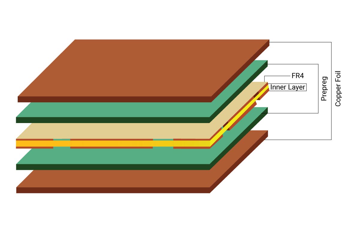
The PCB lamination process occurs at the point in fabrication when the inner layers, foil and prepreg are stacked, heated and pressed into a circuit board. As with many processes in circuit board fabrication, method and materials vary.
PCB Lamination Techniques
A multilayer PCBA is fabricated in various layers, either as thin-etched boards or trace layers that are then bonded with lamination. In this standard process, internal layers are heated intensely and put under pressure prior to high-temperature curing. As the PCB slowly cools, pressure is released before the circuit is laminated with a photosensitive dry resist.
Teflon (PTFE) microwave laminates are commonly used for RF circuit boards with high-speed signal flows. Characteristics like minimal electrical loss, tight depth tolerance, and a reliable dielectric constant, make them ideal PCBAs for applications involving radio frequencies.
Sequential lamination is a popular method when a PCB has two or more subsets. After creating subsets of multi-layered PCBs in a separate process, with an insulating material between each pair, standard PCB lamination processes are then implemented. It should be noted that this method adds time and cost to the build process.
Sequential lamination is a fundamental technique in multilayer circuit board fabrication. The term describes how a PCBA is built up in layers through the use of copper sub-composites and insulating laminate material. It allows for complex tasks to be completed, such as etching routes onto internal copper layers or drilling buried vias. High-density interconnect (HDI) PCBAs, which are increasingly common in electronics, would not be possible without this technique.
The PCB Lamination Process
In circuit board fabrication, lamination follows the application of the inner layer to the PCB. Lamination is similar across all circuit boards that consist of substrate, laminate, solder mask and silkscreen.
Steps in PCB Lamination Process
1.Panels are washed to remove corrosion, dry film, anti-foam residues, dry film stripping and any fingerprints.
2.Micro-etching is performed using a standardized brown or black oxide treatment, which reduces copper thickness. This oxide treatment is used so that the epoxy resin provides better adhesion, while avoiding problems like delamination.
3.The inner layers and prepreg are stacked on the gluing machine, where they are glued together.
4.Once glued, rivets are used–along the unusable board edge– to complete registration and strengthen the PCB, by connecting the inner layer to the prepreg. This strengthens the stack-up, ensuring it will not move during the PCB lamination process. A stainless-steel patch and prepreg sandwiches the copper foil and completes the stack-up.
5.The stack-up is then placed under extreme temperatures, the exact temperature is dependent upon the materials used from the data sheets. Pressures of over 33,000 lbf/ft2 (about 180 tons per square meter) are applied for up to two hours.
6.After exposure to high pressures and temperatures, layers are moved onto a cold press then unmolded and prepared with registration holes using an X-ray machine.
7.Finally, panels are deburred before being rounded at the corners.
The substrate and laminate are essentially the foundation of the circuit board and supply a PCB with its structural integrity. However, laminates themselves may also be used as a core material in some constructions. As with substrates, laminates can be customized to meet specific requirements.
Tensile and shear strength are important in the PCB lamination process as well. The coefficient of thermal expansion (CTE) and glass transition temperature (Tg) both contribute to a circuit board’s reliability. CTE refers to the rate of expansion of PCB material as it is heated, and because the CTE for substrate is much higher than copper, connection issues can develop as the PCB is heated. Tg corresponds to the temperature at which the material within the PCB becomes unstable mechanically.
As substrate and laminate are the foundation on which circuit boards are based, it is important to select the best material. It is this material that will determine the thermal, electrical and mechanical properties of the finished PCBA.
Ensuring Quality During PCB Lamination
Modern electronics have compelled PCBAs to develop exponentially, with users clamoring for lighter weights, higher speeds, better functionality, longer lifecycles, increased reliability and miniaturization. As a result, circuit board lamination can affect a PCBA’s functionality and lifecycle, which is why care should be taken whenever selecting circuit board material.
Dielectrics commonly used for laminates:
FR-4 is the most common material class and represents the default for standard boards. It has a Tg of 135˚C, though versions with higher Tg—from 150-210˚C—are used in high-density applications.
CEM-1 has a Tg of 122˚C and works well in high-density applications.
CEM-2 and CEM-3 have a Tg of 125˚C and also work well in high-density applications
PTFE can be a good choice for high-frequency, high-power and microwave applications, with a Tg of 160˚C.
How a design functions in the real world is often due to what materials or lamination techniques are used. It is for this reason that engineers and designers should take the time to understand the various parts of PCB stack-ups and how they will be used.


