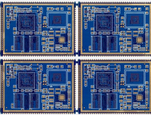
Components that are placed too close to the edge of the board run the risk of being damaged or causing problems with other aspects of circuit board manufacturing. The problem is that some components have to be close to or on the edge of the board in order to perform their function. Connectors, switches, and other system interfaces have to be accessible to both connecting cables and human hands. To place your PCB parts so that they are in the most optimal locations, it is important to understand the concerns of placing components too close to the board edge.
In this article, we’ll look at these potential problems as well as discuss some general PCB component to edge clearance considerations that can help.
Potential Problems without Adequate PCB Component to Edge Clearances
For the best performance of the circuit board, the placement of the components must be optimally arranged for the circuitry. In general, most of the component placement should be more centrally located where the processor and memory chips can interconnect with their associated circuitry. This will also allow these hot devices to distribute their heat more evenly throughout the board. At some point, though, this circuitry will have to send and receive data external to the board, which will require connectors and other interface devices. These components are usually located close to the edge of the board along with their associated circuitry.
Components that are too close to the edge of the board can be victimized by their placement, or in turn, can cause manufacturing problems for the PCB. Here are some general concerns that the designer should be aware of:
-Component location: Connectors on the edge of the board must be placed correctly to interface with their off-board cable or wiring harnesses. Consideration must also be given to these larger components for any possible interference with airflow for cooling, or human access for debugging and rework. Additionally, the associated circuitry of these connector’s also needs to be placed with the component to edge clearance requirements in mind.
-Circuit board assembly: Automated PCB assembly equipment, such as pick & place machines, wave soldering, and solder reflow ovens, all have different transport systems for processing the boards. Components that are placed too close to the edge run the risk of interfering with the different conveyor belts used in the machines. Also, the taller a component is next to the board edge, the more it could potentially interfere with the automated assembly processes. It is a good practice locating larger parts like tall capacitors further back from the edge of the board.
-Component damage: Circuit boards are often batch manufactured in panels and later on have to be broken out of those panels. During depanelization, the circuit board may flex just enough to cause problems for board edge components. Solder joints may crack, and metal pads and traces may lift or break. This kind of damage can be difficult to detect and may lead to intermittent circuitry problems during operation. In addition, components near the edge of the board may interfere with the cutting tools used to break the boards out of the panels.
-Manufacturing fixtures: Circuit boards are often placed in fixtures during manufacturing for both assembly and test. In-circuit test, for instance, the board is held in place with a vacuum drawdown for its probes to firmly contact each test point on the board. This requires enough space around the edge of the board for the test fixture to create the airtight seal it needs for the vacuum to work.
These are some of the problems that PCB layout designers need to be aware of when placing their components next to the edge of the circuit board. Next, we’ll look at some general placement rules that will help to avoid these issues.
Design Rules of Thumb for Placing PCB Components Next to the Board Edge
Although it would be convenient to state definitively what the required component to board edge clearances should be, the truth is that these values vary between manufacturers. What we can do, though, is to lay out the different categories of clearances to be aware of along with some general values that you can use as a starting point:
-Panels with V-grooves: Some circuit boards are separated from their panels by cutting V-grooves along the board outline. To give the cutting tools enough room to work without causing any damage, components should be set back between 0.05 and 0.075 inches from the edge of the board. Taller components, such as electrolytic capacitors, should be set back 0.125 inches from the board edge.
-Panels with breakout tabs: Other circuit boards are routed out of their panels before manufacturing and held in place with breakout tabs until depanelization. These boards should follow the same general board edge clearances as boards that will be cut out, except for parts that are directly next to a tab. In those locations, the components should be set back 0.125 inches from the tab, while taller parts should have a clearance of 0.25 inches.
-Physical support: Some circuit boards require additional support during manufacturing due to the overall size, thickness, and weight of their components. To do this requires a brace that is attached to the panel, and components must not be placed where these braces and needed.
-Copper: Although not a component, there also needs to be enough clearance between traces and power planes to the board edge. This is to protect the metal from twisting and lifting during depanelization. It is recommended to hold the copper back at least 0.02 inches from the board edge and 0.125 inches from a breakout tab.
Drilled Holes: Holes also are not a component, but they need to observe board edge clearance rules as well. It is recommended to maintain a minimum distance of 0.02 inches between the edge of the hole and the edge of the board. That distance should be doubled if the board is going to be cut out of the panel using the V-groove method.
-Test points: ICT test points also need to be kept back from the edge of the board by 0.1 inches. This will ensure that there is enough room around the perimeter of the board for the vacuum seal of the test fixture.


