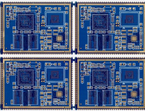
After the PCB board layout design is completed, it is necessary to carefully check whether the wiring design meets the rules set by the designer, and also to confirm whether the established rules meet the requirements of the PCB board production process.
After the general PCB board layout design is completed, you need to check the following aspects:
1. Line and line, line and component pad, wire and through hole, component pad and through hole, whether the distance between the through hole and the through hole is reasonable, and whether the production requirements are met.
2. Is the width of the power and ground wires appropriate? Is there a tight coupling between the power supply and the ground (low wave impedance)? Is there a place in the PCB that allows the ground wire to be widened?
3. Whether the best measures are taken for the key signal lines, such as the shortest length, the added protection line, the input line and the output line are clearly separated.
4. Whether the analog circuit and the digital circuit part have separate ground lines.
5. Whether the graphics (such as icons and annotations) added to the PCB board will cause a signal short circuit. Modify some undesired line shapes.
6. Whether the process line is added on the PCB, whether the solder mask meets the requirements of the production process, whether the solder mask size is appropriate, and whether the character mark is pressed on the device pad, so as not to affect the assembly quality of the circuit board.
7. Whether the edge of the outer frame of the power supply layer in the multilayer PCB board is reduced, for example, the copper foil of the power supply ground layer is likely to cause a short circuit outside the exposed plate.


