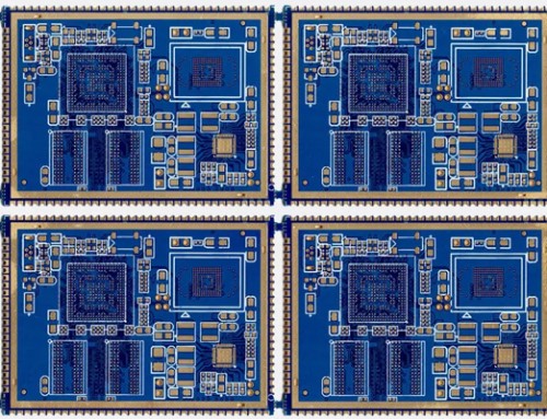
The success of PCB manufacturing lies on the reliability and consistency of the process. To achieve this, strict tolerances must be maintained throughout the manufacturing process. In the world of PCB fabrication, tolerance refers to the amount of allowable deviation from a specified value. For example, a PCB trace width might have a tolerance of +/- 0.005 inches, This means that the width of the trace can vary by up to 0.005 inches. Tolerance is important in PCB fabrication because it ensures that components will fit properly and that the finished product will function as intended, There are a variety of factors that can affect tolerance, including material properties, manufacturing processes, and design specifications. Needless to say, maintaining tolerance is critical to the success of the PCB manufacturing process.
As technology advances, the standards for printed circuit board (PCB) manufacturing become more demanding, To meet these standards, manufacturers must have a keen understanding of the different elements of PCB manufacturing and the required tolerances for each. In this post, we will explore the different elements of PCB manufacturing and the required tolerances for each.
A Note Before Getting Started
Tolerances may vary across manufacturers. The degree of precision when creating alignment holes, for example, will vary from one manufacturer to the next. The same is true for the width of copper traces and the thickness of the finished board.
When fabricating a PCB, it’s important to know the tolerance levels of the manufacturer you’re working with. This will ensure that your board meets the necessary specifications and performs as expected.
Circuit Board Dimensional Tolerances
There are many things to consider when manufacturing a printed circuit board (PCB). From the material to the design, each element must be carefully chosen to ensure the final product is up to the mark. But what are the specific tolerances that must be met in order for a PCB to be successful? We will now explore the different elements of PCB manufacturing and the required tolerances for each.
Circuit Board Thickness: Fabricating PCBs with the right thickness is critical to its performance. The tolerance, or allowable variation, in thickness is therefore an important consideration. There are two main reasons why the thickness of a PCB is critical. The standard tolerance for the thickness of a PCB is ±10%. This means that the PCB can be up to 10% thicker or 10% thinner than the specified thickness and still be within specification.
Drilling Tolerance: Drilling a printed circuit board (PCB) is an important part of the manufacturing process, but it is also one of the most difficult and challenging tasks. This is because PCBs are extremely thin and fragile, and even the slightest mistake can ruin the entire board. That’s why it’s so important to have a high degree of tolerance when drilling PCBs. The tolerance is typically given in terms of the width of the hole that is being drilled. For example, a tolerance of +/- 0.005 inches means that the hole must be drilled within 0.005 inches of the desired width in order to be considered accurate.
Routing Tolerances: When designing a PCB, it is important to consider the routing tolerance of the board. The routing tolerance is the minimum amount of space that must be between two conductors on the board. If the space between the conductors is too small, the circuit will not function properly. There are a variety of factors that can affect the routing tolerance of a PCB, including the width of the traces, the spacing between the traces, and the thickness of the board.
Copper Thickness: The thickness of the copper on a PCB must be within a certain tolerance in order for the board to function properly. This tolerance is typically plus or minus 10% of the specified thickness. For example, if the specified thickness is 1 ounce, the tolerance would be plus or minus 0.1 ounce. The thickness of the copper is important because it determines the amount of current that can flow through the PCB. If the copper is too thin, the current will be too low and the PCB will not function properly. If the copper is too thick, the current will be too high and the board could be damaged.


