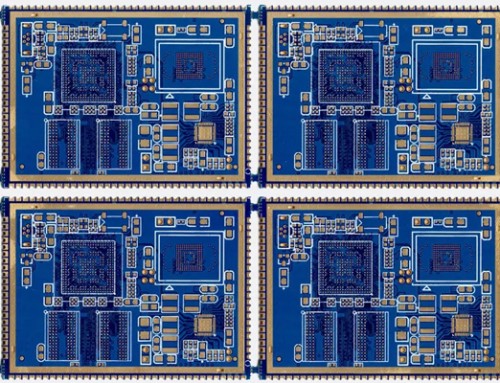
Today, most PCBs can be considered to be at risk of some type of signal integrity problem that is normally associated with high speed digital design. High speed PCB design and layout focuses on creating circuit board designs that are less susceptible to signal integrity, power integrity, and EMI/EMC problems. While no design is ever totally free of these problems, by following these high speed board design guidelines they can be reduced to the point where they are unnoticeable and do not create performance problems in the final product.
High Speed Digital Design Basics
So what is high speed board design? High speed design specifically refers to systems that use high speed digital signals to pass data between components. The dividing line between a high speed digital design and a simple circuit board with slower digital protocols is blurry. The general metric used to denote a particular system as “high speed” is the edge rate (or rise time) of digital signals used in the system. Most digital designs use both high speed (fast edge rate) and low speed (slow edge rate) digital protocols. In today’s era of embedded computing and IoT, most high speed circuit boards have an RF front end for wireless communication and networking. Although all designs begin from a schematic, a major part of high speed PCB design is focused in interconnect design, PCB stackup design, and routing.
Planning Your High Speed PCB Stackup and Impedance
The PCB stackup you create for a high speed circuit board will determine the impedance, as well as ease of routing. All PCB stackups include a set of layers dedicated to high speed signal, power, and ground planes, and there are several points to consider when assigning layers in a stackup:
Board size and net count: How large will the board be and how many nets do you need to route in the PCB layout. Physically larger boards might have enough space to allow you to route throughout the PCB layout without using more than a few signal layers.
Routing density: In the case where net counts are high and the board size is constrained to a small region, you may not have a lot of room for routing around the surface layer. Therefore, you’ll need more internal signal layers when traces are pushed closer together. Going to a smaller board size can force higher routing density.
Number of interfaces: Sometimes it’s a good strategy to route only one or two interfaces per layer, depending on the width of the bus (series vs. parallel) and the board size. Keeping all signals in a high speed digital interface on the same layer ensures consistent impedance and skew is seen by all signals.
Low speed and RF signals: Will there be any low speed digital or RF signals in your digital design? If so, these may take up space on the surface layer that could be used for a high speed bus or components, and an additional internal layer might be required.
Power integrity: One of the cornerstones of power integrity is the use of a large power plane and ground plane for each voltage level required in your large ICs. These should be placed on adjacent layers to help ensure there is high plane capacitance to support stable power with decoupling capacitors.
PCB Material Options, Layer Count, and Thickness
Before designing your PCB stackup, consider the layer count needed to accommodate all digital signals in your design. There are several ways to determine this, but these methods rely on a bit of math and some past experience in high speed board design. In addition to the points listed above for considering layer count, large high speed ICs with BGA/LGA footprints can dictate the required board size. When doing BGA fanout, you can generally fit 2 rows per signal layer, and make sure to include the power and ground plane layers in your layer count when building a stackup.
FR4-grade materials can generally be used in a high speed digital design as long as the routes between components are not too long. If routes do become too long, there will be too much loss in your high speed channel, and components on the receiver end of the channel may not be able to recover signals. The primary material property to consider when selecting materials is the loss tangent of your PCB laminates. The channel geometry will also determine losses, but generally opting for a lower loss tangent FR4 laminate is a good place to start in smaller boards.
If your routes are too long, then a more specialized material might be needed as the substrate for your high speed signals. PTFE-based laminates, spread glass laminates, or other specialized material systems are a good choice to support larger high speed digital boards, where routes are very long and low insertion loss is required. A good entry-level high-Tg set of laminate materials for small-sized high speed PCBs is 370HR. For larger boards, something like Megtron or Duroid laminates are good options.


