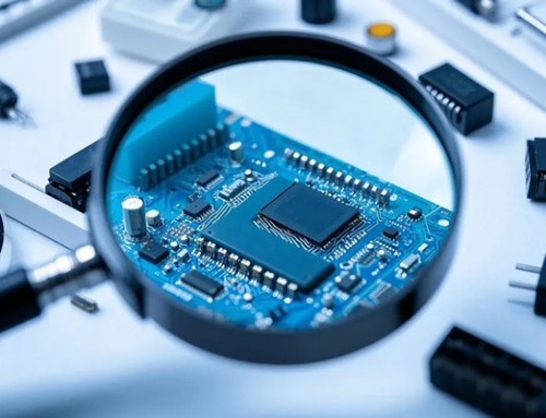
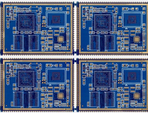
High-Density Interconnect (HDI) PCBs have revolutionized the electronics industry by offering a solution to the challenges posed by high-density applications. With the increasing demand for smaller, lighter, and more powerful electronic devices, HDI PCBs have become an essential part in enabling the creation of intricate and complex circuits. This article will delve into the capabilities of HDI PCBs and discuss their significance in various high-density applications.
What are HDI PCBs? HDI PCBs, also known as double-sided or multilayer printed circuit boards, are designed to provide a high degree of interconnectivity in a compact form factor. They achieve this by incorporating microvias, which are tiny holes drilled through the board’s layers, allowing for the routing of conductors between layers. This technology enables the creation of dense and intricate circuits, making them ideal for high-density applications.
Advantages of HDI PCBs for High-Density Applications
a. Increased Density: HDI PCBs offer a higher density of interconnections, allowing for more components to be mounted on a smaller board surface area. This is particularly crucial for applications such as smartphones, wearables, and other portable devices, where space is at a premium.
b. Reduced Size and Weight: The compact nature of HDI PCBs enables the creation of smaller and lighter electronic devices. This is especially important in industries such as aerospace and defense, where weight reduction is a critical factor.
c. Improved Electrical Performance: The use of microvias in HDI PCBs allows for precise and controlled routing of conductors, resulting in improved electrical performance. This is essential for applications that require high-speed data transmission, such as computer boards and communication systems.
d. Enhanced Reliability: HDI PCBs are designed with precision and care, ensuring reliable connections and reducing the risk of failures. This is crucial for high-stakes applications like medical devices and industrial control systems.
HDI PCB Assembly Process
The assembly of HDI PCBs involves several steps, including design, fabrication, and manufacturing. The design phase focuses on creating a layout that optimizes the interconnections while considering the constraints of the application. The fabrication process involves the creation of microvias and the deposition of conductive layers, while the manufacturing process includes plating, drilling, and lamination.
Applications of HDI PCBs in High-Density Electronics
a.Smartphones and Tablets: HDI PCBs are extensively used in smartphones and tablets to accommodate the numerous components and high-speed data connections required for these devices.
b. Wearable Electronics: The compact size and lightweight nature of HDI PCBs make them ideal for wearable devices, such as smartwatches and fitness trackers, where space is limited.
c. Aerospace and Defense: HDI PCBs are used in aerospace and defense applications to reduce weight and increase the reliability of electronic systems, which are crucial in critical situations.
d. Medical Devices: The precise and controlled interconnections provided by HDI PCBs are essential for medical devices, where reliability and performance are paramount.
e. Computer Boards and Communication Systems: High-speed data transmission and increased density are key requirements for computer boards and communication systems, making HDI PCBs an excellent choice.
HDI PCBs have emerged as a game-changer in the electronics industry, enabling the creation of high-density applications that were once considered impossible. With their increased density, reduced size and weight, improved electrical performance, and enhanced reliability, HDI PCBs have become an indispensable part in various industries. As technology continues to advance, the capabilities of HDI PCBs are likely to expand further, enabling the development of even more sophisticated and compact electronic devices.


