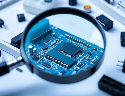
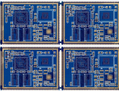
Printed Circuit Boards (PCBs) are an integral part of modern electronic devices, providing a platform for the connection and integration of various electronic components. With the advancement in technology, the demand for smaller, more complex, and efficient electronic devices has increased. To meet these demands, multi-layer PCBs have become prevalent. This article discusses the methods to improve circuit wiring density in multi-layer PCBs and highlights their advantages.
Utilizing Multi-layer PCBs: Multi-layer PCBs consist of two or more conductive layers separated by insulating layers. The number of layers in a multi-layer PCB can vary depending on the design requirements. The layers are connected through vias, which are holes drilled through the PCB and plated with conductive material. The use of multi-layer PCBs allows for increased circuit density, reduced space requirements, and improved signal integrity.
Techniques to Improve Wiring Density
To enhance the circuit wiring density in multi-layer PCBs, several techniques can be employed:
a. Blind and Buried Vias: Blind vias are connecting holes that connect the outer layers of the PCB to an internal layer without extending through the entire board. Buried vias, on the other hand, connect internal layers without connecting to any external layers. The use of blind and buried vias enables more efficient use of space and allows for increased wiring density.
b. Microvias: Microvias are small-diameter vias that provide connections between layers in multi-layer PCBs. They have a smaller impact on the circuit routing and can be placed closer to each other, thus increasing the wiring density. Microvias also help in reducing signal delay and improving overall signal integrity.
c. High-density Interconnect Technology (HDI): HDI PCBs incorporate advanced technologies such as microvias, laser drilling, and stacked vias to achieve higher wiring density. HDI PCBs have finer trace widths and spaces, allowing for more complex and dense circuit designs.
d. Optimized Layer Stack-up: Optimizing the layer stack-up of multi-layer PCBs can also contribute to increased wiring density. By carefully planning the placement of signal, power, and ground layers, designers can minimize the space between layers and increase the number of routing channels.
Advantages of Improved Wiring Density
Enhancing the circuit wiring density in multi-layer PCBs offers several advantages:
a. Reduced Space Requirements: With increased wiring density, the overall size of the PCB can be reduced, making it suitable for compact electronic devices. This is particularly important in applications such as smartphones, wearables, and other portable devices.
b. Improved Signal Integrity: High wiring density allows for shorter trace lengths, reducing signal delays and crosstalk between traces. This results in improved signal integrity and better overall performance of the electronic device.
c. Enhanced Thermal Management: Multi-layer PCBs with improved wiring density can accommodate additional thermal management features such as embedded heat sinks or thermal vias. These features help dissipate heat more efficiently, ensuring the reliable operation of the electronic device.
d. Increased Component Density: With higher wiring density, more components can be placed on the PCB, leading to increased component density. This enables the design of more complex and feature-rich electronic devices.
Improving the circuit wiring density in multi-layer PCBs is essential to meet the growing demands of smaller, more complex, and efficient electronic devices. By utilizing techniques such as blind and buried vias, microvias, HDI technology, and optimized layer stack-up, designers can achieve higher wiring density. The advantages of enhanced wiring density include reduced space requirements, improved signal integrity, enhanced thermal management, and increased component density. As technology continues to evolve, the importance of these techniques and their benefits in multi-layer PCB design will only grow.


