
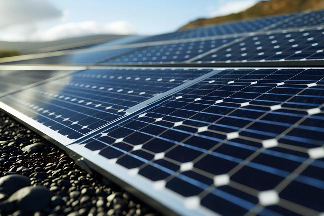
Energy storage systems are becoming increasingly important in various applications such as renewable energy, electric vehicles, and grid storage. The printed circuit board (PCB) layout plays a crucial role in the performance and reliability of energy storage systems. In this article, we will discuss the key considerations for PCB layout in energy storage systems and the manufacturing difficulties associated with them.
Power and Signal Integrity: Power integrity is a critical aspect of energy storage PCB layout. The PCB must be designed to minimize power loss and ensure efficient power distribution. This involves careful selection of conductors, trace width, and spacing to reduce resistance and inductance. Signal integrity is also important to ensure accurate and reliable communication between components. Proper grounding and shielding techniques should be employed to minimize noise and interference.
Thermal Management: Thermal management is a significant concern in energy storage systems, as high temperatures can degrade the performance and lifespan of the system. The PCB layout should facilitate efficient heat dissipation by providing adequate space around heat-generating components and using appropriate cooling techniques such as ventilation or heat sinks. Thermal vias can also be incorporated into the PCB design to improve thermal conductivity.
Electrochemical Considerations: Energy storage systems involve electrochemical processes, which can have implications for PCB layout. The layout should minimize the risk of short-circuits and electrochemical reactions between different cells or electrodes. This can be achieved by using isolation techniques such as insulating materials or epoxy potting. Additionally, the PCB should be designed to withstand the harsh environment of the energy storage system, including exposure to chemicals and moisture.
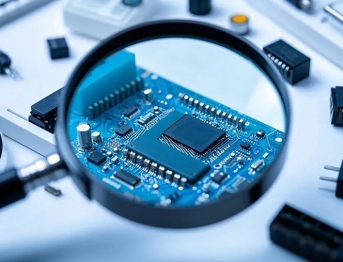
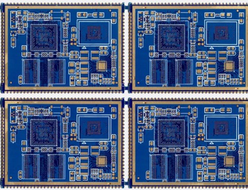
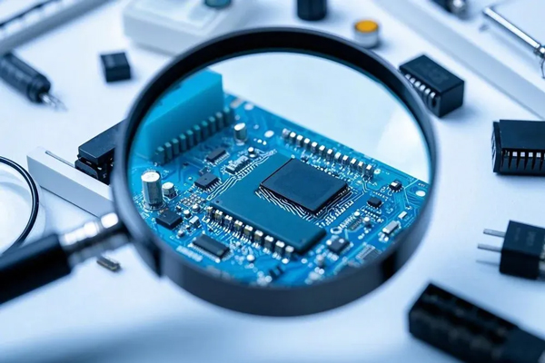
Manufacturability: Manufacturing energy storage PCBs can be challenging due to the complexity of the designs and the requirement for high precision. The manufacturing process must be capable of handling the intricate features and fine pitches involved in energy storage PCBs. Automated manufacturing techniques such as lithography and etching are often used for high-density interconnects. However, manual assembly processes may still be required for certain components or assembly steps.
Assembly and Integration: Energy storage systems often require the integration of multiple components such as battery cells, power electronics, and control circuits. The PCB layout should facilitate easy assembly and integration of these components. This may involve the use of through-hole or surface-mount technology (SMT) components, depending on the design requirements. Proper design and documentation are essential to ensure efficient assembly and minimize the risk of errors.
Reliability and Durability: The PCB layout should be designed with reliability and durability in mind, considering the demanding operating conditions of energy storage systems. This involves using robust materials and design techniques to withstand mechanical stress, temperature variations, and electrical cycling. Compliance with industry standards and regulations is also crucial to ensure the safety and reliability of the energy storage system.
Energy storage PCB layout requires careful consideration of power and signal integrity, thermal management, electrochemical considerations, manufacturability, assembly and integration, and reliability. Addressing these considerations and overcoming manufacturing difficulties is essential to ensure the optimal performance and longevity of energy storage systems. Close collaboration between PCB designers, manufacturers, and system engineers is necessary to develop robust and efficient energy storage PCB solutions.