
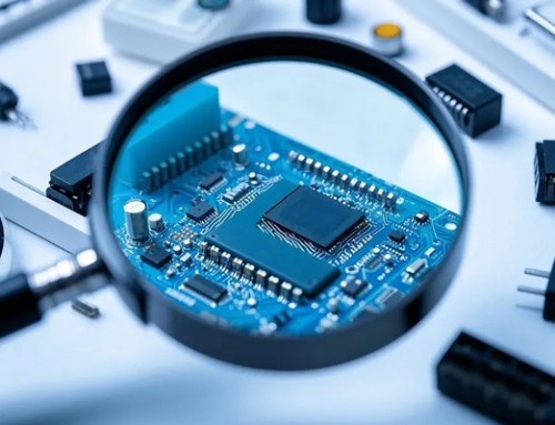
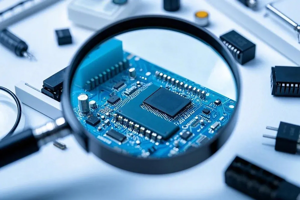
In the realm of printed circuit board (PCB) manufacturing, optimizing material utilization is a critical aspect that directly influrnces production costs and efficiency. PCB panel design, the process of arranging multiple PCBs on a single sheet of material, plays a pivotal role in this optimization. This article delves into various techniques and strategies that can be employed to enhance material utilization in PCB panel design, thereby reducing waste and lowering production costs.
1. Understanding PCB Panel Design
PCB panel design involves the strategic arrangement of multiple PCBs on a single panel, often referred to as a “nest.” The primary objective is to maximize the number of PCBs that can be fabricated from a given sheet of material, while minimizing waste. This process requires a careful balance between PCB layout, panel size, and manufacturing constraints.
2. Standard Panel Sizes and Shapes
Utilizing standard panel sizes and shapes is a fundamental technique to improve material utilization. Standard panels, such as 18″x24″ or 20″x24″, are commonly used in the industry and are designed to fit efficiently on manufacturing equipment. By adhering to these standards, designers can minimize the amount of material lost during the cutting process.
3. Efficient PCB Layout
The layout of individual PCBs within the panel is crucial for maximizing material utilization. Here are some key considerations:
Rectangular and Compact Designs: Rectangular PCBs with compact designs tend to nest more efficiently than irregularly shaped ones.
Uniform Orientation: Aligning PCBs in the same orientation can simplify the manufacturing process and reduce setup time.
Minimizing Board-to-Board Spacing: Reducing the spacing between PCBs can significantly increase the number of boards per panel. However, sufficient spacing is necessary to ensure proper routing and avoid electrical interference.
4. Nested and Clustered Panels
Nested and clustered panel designs are advanced techniques that can further enhance material utilization:
Nested Panels: This approach involves arranging PCBs of different shapes and sizes within the same panel. Computer-aided design (CAD) software can be used to optimize the nesting process, ensuring minimal waste.
Clustered Panels: In this method, multiple identical PCBs are grouped together in a cluster, which can then be replicated across the panel. This approach is particularly effective for high-volume production runs.
5. Utilizing Panel Routing and V-scoring
Panel routing and V-scoring are two common methods used to separate individual PCBs from the panel:
Panel Routing: This involves cutting a path around the perimeter of each PCB. By carefully planning the routing paths, designers can minimize the amount of material removed during the process.
V-scoring: V-scoring creates a V-shaped groove along the edges of the PCBs, allowing them to be easily snapped apart. This method can save material compared to traditional routing.
6. Implementing Design for Manufacturing (DFM) Principles
Design for Manufacturing (DFM) principles are essential for optimizing PCB panel design:
Minimizing Complexities: Simplifying the design by reducing the number of layers, vias, and complex geometries can make the paneling process more efficient.
Standardizing Components: Using standard components and footprints can facilitate easier assembly and reduce the risk of errors.
Collaboration with Manufacturers: Working closely with PCB manufacturers to understand their capabilities and constraints can lead to more efficient panel designs.
7. Leveraging Software Tools
Modern CAD software offers a plethora of tools and features specifically designed for PCB panel optimization:
Automatic Nesting: CAD software can automatically arrange PCBs on a panel to maximize material utilization.
Simulation and Analysis: Simulating the manufacturing process can help identify potential issues and optimize the panel design accordingly.
Real-time Feedback: Some software tools provide real-time feedback on material utilization, allowing designers to make adjustments on the fly.
8. Continuous Improvement and Feedback Loop
Establishing a continuous improvement and feedback loop is vital for ongoing optimization:
Post-Production Analysis: Analyzing the results of each production run can reveal opportunities for further optimization.
Collaborative Feedback: Encouraging feedback from designers, manufacturers, and assembly teams can lead to innovative solutions and improvements.
Benchmarking and Best Practices: Benchmarking against industry standards and adopting best practices can drive continuous improvement in material utilization.
PCB panel design is a complex but essential aspect of PCB manufacturing. By employing the techniques and strategies outlined in this article, designers can significantly enhance material utilization, reduce waste, and lower production costs. Continuous improvement, collaboration, and the use of advanced software tools are key to achieving optimal panel designs in an ever-evolving industry. As technology advances and manufacturing processes evolve, the quest for greater efficiency in PCB panel design will remain a pivotal focus for the electronics industry.