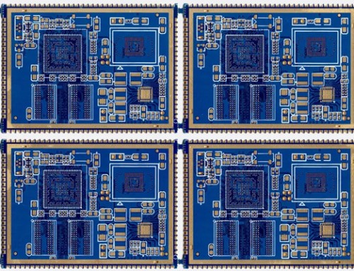
What is a Ball Grid Array (BGA) Packaging Technology?
BGA is a surface-mount technology that uses an array of solder balls for electrical interconnection. The interconnection is achieved between the package body and the base. Based on different packaging materials, a number of BGA components has been developed such as Ceramic BGA (CBGA), Plastic BGA (PBGA), Tape BGA (TBGA), Ceramic Column (CCBGA), and Chip-Scale Package (CSP). Some of the features offered by aforementioned BGA components include higher packaging reliability, lower soldering defects, and more solid soldering joints; higher number of I/O ends and large I/O end spacing, excellent electrical and frequency characteristics, and guaranteed BGA soldering planarity.
The importance of the right PCB layout cannot be overemphasized. While it connects various electronic components on a single substrate, it is the method by which components are attached to the board’s surface that can go a long way in affecting its stability as also its efficiency.
A Pin-grid array, popularly referred to as PGA, was by far the standard in packaging integrated circuits on a board. The same, however, has now been replaced by the Ball Grid Array or BGA design. Simply put, while the PGA used a square arrangement of pins to mount components, BGA replaces pins with metal balls made of solder attached to the underside of the unit.
A typical integrated circuit designed with BGA comprises of a chip or processor that is attached to the substrate. The die in turn is connected to the slab through a wire. Solder balls are then attached to the other side of the substrate. The ready component is now referred to as a package. The package then is fastened to a circuit board by way of the use of solder.
Advantages of BGA
There are several advantages of using BGA, primary among them being:
• Lower track density- With metallic solder balls arranged in a grid like pattern. Track densities can be significantly reduced. In turn what it means is an optimized pcb layout as the closeness of balls increases the efficiency. Trying to do the same with a Pin Grid Array, by increasing the volume of pins enhances the risk of accidental bridging. In case of BGA, however, with the balls made of solder, bridging isn’t that much of a concern.
• Reduced chances of component damage- A pin grid array requires a soldering process that has chances of damaging the component. On the other hand, with BGA, the solder balls only need to be heated so that they melt and adhere to the PCB. The chances of any component damage, is therefore significantly reduced. Also, the surface tension between the ball and the circuit board ensure that the package is held in place.
• Reliability- With the use of PGA, the fragility of the pins was always an issue. They require extreme care and are prone to being bent and damaged. With BGA using solder pads connected to solder balls, the system is far more robust and reliable
• Improved performance- On account of the grid array the connections inside the BGA are shorter. What it translates into is reduction of lead induction level leading to improved performance typically at higher speeds.
• Lower incidence of overheating- Reduced heat resistance between the BGA and the circuit board offer a major advantage. In fact, the heat generated dissipates into the circuit board as the BGA units provide thermal channels to direct the heat away.
This however, is not to suggest that the ball grid array does not come with its own set of issues. Primary among them, being the inflexibility of the balls! In fact, the rigid bond between the board and the component can result in physical stress, which in turn can impact efficiency. Also on account of the proximity between the board and its components, it can be quite a task to make a thorough check of the quality aspects of the PCB. Also, it is not easy to rework boards that contain BGAs unless the correct equipment is available. A faulty BGA will therefore need to be removed by locally melting the device. Great care is needed to see that other devices in the vicinity aren’t affected or damaged. Once removed, of course the BGA can be replaced with a new one.
There could therefore be a number of applications where BGA isn’t the best alternative. In such cases a variation of the standard BGA, called PBGA or Plastic Ball Grid Array is used. It has a plastic-coated body, a substrate that is glass mixture laminated and has copper traces. What it does for the system is that it displays increased stability as far as temperature is concerned. Also, it uses pre-formed solder balls that can be reshaped. There are also a whole lot of other BGA types that can be used in different situations- important among them are:
• Moulded Array Process Ball Grid Array or what is called MAPBGA, this is ideal for low to mid performance devices that comes at a low cost.
• Thermally Enhanced Plastic Ball Grid Array or TEPBGA, this package provides for high heat dissipation levels.
• Tape Ball Grid Array or TBGA, this is ideal for mid to high-end solutions.
• Package on Package or PoP, this allows for stacking a memory package on top of a base device and hence is useful for applications where space is a real constraint.


