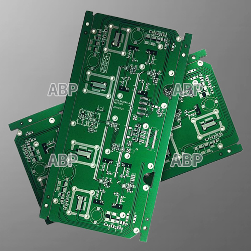
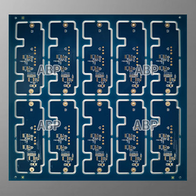
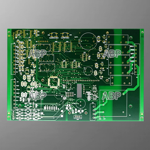
With many advantages adding to cost reduction and ease of product assembly, flexible circuit board is increasingly becoming popular in the marketing, that numerous people in want of more information about flexible circuit boards.
What are Flexible PCBs?
Flexible PCBs are members of electronic and interconnection family. They consist of a thin insulating polymer film having conductive circuit patterns affixed thereto and typically supplied with a thin polymer coating to protect the conductor circuits.
What are Rigid flexible PCBs?
Rigid flexible PCBs can have circuit boards both externally and internally. They consist of multiple inner layers of flexible circuits. Rigid flexible circuits contain more materials than flexible circuits. The materials include rolled annealed copper, electro deposited copper, epoxy, acrylic, pre-preg, pressure sensitive, adhesiveless base material, FR-4, polyimide, polyester, solder mask, flexible solder mask, and photo image-able cover lay. Rigid flexible circuits are found in many electronic areas, such as, in the industrial field and the medical field.
Advantage of Flexible PCB
Decreased assembly time and costs and reduction of assembly error
More design freedom and flexibility during installation
High density applications and improved airflow
Increased heat dissipation and system reliability
Potential to replace multiple rigid boards or connectors
Ideal for dynamic or high-flex applications
Stacked FPCs are perfect at various configurations
Disadvantages of Flexible PCB
Cost increase over rigid PCBs
Increased risk of damage during handling or use
More difficult for repair and rework
Flexible PCB Constructions
There are four main types of flexible circuit constructions and their application.
Single-Sided or Single-Layer Flex PCB:
Single layer conductor (usually copper) bonded to a dielectric film
Basic construction allows component connections to one side only
Chemical etching forms designed circuit patterns, and a polyimide overlay is used to environmentally seal component traces
Most economical flex circuit construction
Many applications in automotive lighting, consumer devices and other cost-sensitive, high-volume applications where dynamic flex and thickness profile are required, but circuitry design isn’t complex.
Double-Sided Flex PCB:
Two conductor layers of copper, double side bonded to a dielectric film
Versatile construction can be customized to match physical and electrical application needs by varying copper type and thickness, and dielectric insulator thickness
Plated thru-holes provide layer conductivity with double-sided solder connection compatibility
Primarily used in bend-to-install applications due to dynamic flex capabilities provided by thin core construction and rolled-annealed copper conductors
Cost to manufacture is higher than rigid PCB due to pattern loss and manual assembly of customized designs. Upsides include improved power/ground integration, 3D flex and vibration resistance.
Multi-Layer Flex PCB:
Three or more conductive layers combining multiple double sided or single sided circuits to create complex interconnection designs with required electrical shielding, often using surface mount technologies
Higher cost due to multiple lamination steps required to bond layers together
Specialized fabrication of discontinuous bonding in key areas allows for maximum flexibility while maintaining advanced properties such as impedance and crosstalk control.
Common applications include connector cabling for medical/industrial applications and antenna flex.
Rigid Flex PCB:
Traditionally used in military/aerospace applications for highly specialized and demanding needs.
Recent uses for industrial and commercial designs.
Hybrid of both rigid and flexible circuitry for applications where extra support is needed in the core board area, but also requiring flexible capability in some areas
Conductors in both rigid and flex areas are connected via plated thru holes across multiple layers
Frequently exceeds 15 layers
Often applied in low volume, mission critical applications due to its high cost.
To know more about Flexible Circuit Board, please contact us via [email protected].
| Item | Capability |
|---|---|
| Layers | 1-30 |
| Thicker Copper | 1-6OZ |
| Products Type | HF(High-Frequency)&(Radio Frequency) board, Impedance controlled board , HDI board ,
BGA& Fine Pitch board |
| Solder Mask | Nanya&Taiyo ;LPI & Matt Red, green, yellow,white, blue,black. |
| Base material | FR4(Shengyi China、ITEQ, KB A+,HZ), HI-TG, FR06, Rogers,Taconic、Argon and so on |
| Finished Surface | Conventional HASL,Lead-free HASL,Falsh Gold, ENIG (Immersion Gold)OSP(Entek), Immersion Tin,ImmersionSilver,Hard Gold |
| Selective Surface Treatment | ENIG(immersion Gold)+OSP, ENIG(immersion Gold)+Gold Finger,Flash Gold +Gold Finger,
immersion Silver+ Gold Finger, Immersion Tin+Gold Finger |
| Technical Specification | Minimum line width/gap:3.5/4mil(laser drill) Minimum hole size:0.15mm(mechanical drill)/4mil(laser drill) Minimum Annular Ring: 4mil Max Copper thickness: 6OZ Max Production size:900×1200mm Board Thickness:D/S: 0.2-7.0mm, Multilayers:0.40-7.0mm, Min Solder Mask Bridge:0.08mm Aspect ratio: 15:1 Plugging Visa capability: 0.2-0.8mm |
| Tolerance | Plated holes Tolerance:0.08mm(min±0.05) Non-plated hole tolerance:0.05min(min+0/-0.05mm or +0.05/-0mm) Outline Tolerance:0.15min(min±0.10mm) Functional test : Insulating resistance : 50 ohms (mormality) Peel off strength: 1.4N/mm Thermal Stress test :2650c,20 seconds Solder mask hardness:6H E-Test voltage :500V+15/-0V 30S Warp and Twist: 0.7% (semiconductor test board≤0.3% ) |


