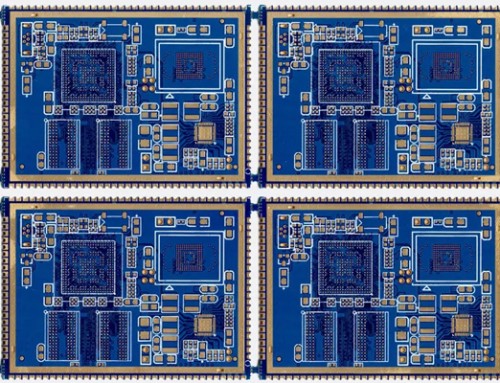
What is a PCB panel?
A PCB panel, also called a PCB array, is a single board consisting of multiple individual boards. Once assembled, the panel is then broken apart, or depanelized, into the individual PCBs during the breakout process. The benefit of the printed circuit board panelization process is a decrease in defeats as automated assembly machines tend to encounter fewer problems during the assembly process. In addition, panelization also reduces cost by improving throughput.
Successful PCB panelization requires multiple design specifications to work properly, including considerations surrounding panelization methods. We’ll detail these panelization methods and their specific requirements more thoroughly in this set of PCB panelization guidelines.
Panelization methods
Multiple panelization methods exist, each with its own drawbacks and benefits. The design of the boards on the panel and the panel itself will often play a large role in which paneliztion methods best suits the application. The most notable of these factors include:
1. Design: The design of the board plays the largest part in determining the most appropriate panelization method. The amount of clearance between components and edge of the board may make certain methods much less suitable than others, as does the presence of edge-hanging components.
2. Components: The types of components used on the board are just as important as their placement. Particularly sensitive components and connectors may play a factor in the most appropriate breakout and panelization method.
3. Materials: The materials used in a PCB may limit which type of panelization method is most appropriate, as some materials are more prone to splintering during the breakout process. Board thickness is also a factor, as particularly thin boards may be more likely to break during assembly, and thick boards may prove more problematic during the breakout process.
These factors limit the choice available to any one application. In fact, many assembly companies may use a combination of methods on any one project to ensure the structural integrity of the array while still mitigating issues during the breakout process.
There are three panelization tecniques in use today, though only two are commonly practiced. They are:
1.V-Sore Panelization: This common method of panelization separates individual PCBs with V-shaped grooves remove approximately a third of the board’s thickness from the top and bottom of the board with an angled blade. A machine is commonly used to finish the breakout process, considering the remaining third of the board between the grooves is surprisingly strong, and hand-breaking can put stress on the PCB and surrounding components.
2. Tab Routing Panelization: PCB arrays that can’t feasibly use a V-groove method will instead use a tab routing method. With this method, PCBs are pre-cut from the array and held in place on the board with perforated tabs. Three to five holes are often used in these perforation patterns. This method is often beneficial for its ability to support designs with edge-hanging components. It can also be broken by hand instead of with tools.
3. Solid Tab Panelization: Arrays can be designed with solid tabs between each board, improving overall strength. However, the depaneling method for this type of panel requires either a depaneling router, a laser-cutting machine or a hook-shaped blade tool. The router can result in dust and vibration, while the laser-cutter is extremely expensive and ineffective on boards over 1mm thick. The hook-bladed option is less expensive but inefficient and prone to blade rotation. This method tends to be less common than the other two.
V-Score and Tab Routing are the preferred panelization methods for most applications. The most important thing for PCB designers is understanding which of the two methods is best for their application. The next step is to design their array for maximal strength and breakout success.
Many prefer the V-groove panelization method when possible for its efficiency and reduction in surface stress. Depaneling machines for this type of array are also relatively inexpensive and cost-efficient. Even better, they’re portable and require minimal maintenance. Though the method tends to result in rougher board edges, this is rarely a concern for applications where V-groove panelization is used.
However, while V-groove panelization is preferable for various applications, it is rather restrictive in terms of panel design. For example, V-groove panelization is not ideal for designs where components are placed too close to or hang over an edge. They also introduce various manufacturing concerns that must be considered during the design process, such as:
1. Clearance: To ensure components are not affected during the cutting process, a clearance of 0.05 inches must be maintained between components and any V-grooves. Taller components may need to be placed further away to ensure the cutter doesn’t interfere with them. For example, surface-mounted multilayer ceramic chip capacitors must be kept at least 1/8 inches away from the score line. Components with larger connection areas should also be placed further away from the groove, as the stress of depanelization can fracture solder joints if they’re placed too close to the V-groove.
2. Jump-Scoring: V-grooves can reduce the structural integrity of a PCB array, causing the leading and trailing edges to sag when run through a wave-solder machine. This can cause the array to warp or get caught in the wave-solder machine. To strengthen an array and prevent these issues, designers can add jump scoring to the leading and trailing edges of the array. This can be accomplished by including a ½ inch breakaway edge on the leading and trailing array edges and running the V-groove approximately halfway through these edges. Just instruct depaneling operators to remove these breakaway edges before separating the boards.
If these design considerations are kept in mind, a V-scored panel should experience minimal problems during the manufacturing and assembly process.


