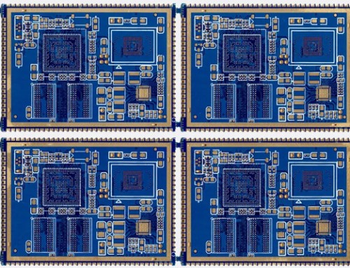
As we all know, an incorrect component placement during PCB assembly can create problems for the completed circuit board ranging from performance to manufacturability. Because these SMT placement issues can manifest themselves in vastly different ways, we will generalize them in the following eight categories:
1. Signal integrity
SMT components that are not placed correctly for their circuits can create signal integrity problems leading to decreased performance or outright failure of the board. PCB layout designers must place their parts according to the signal paths depicted in the schematics and keep digital and analog parts isolated in their design partitions. It is also important to place parts in such a way as to allow for clear signal return paths on the reference plane.
2. Power integrity
Another important consideration for circuit board performance is its power integrity. Bypass capacitors must be placed close to their supply pins to reduce the chance of noise being created in the power delivery network. Power supply components need to be placed tightly together on the same board layer to keep their connecting traces short and reduce inductance in the line.
3. PCB assembly rework
Part of the PCB manufacturing process includes reworking a board during assembly, whether it is an inspection or actual repair or replacement of parts. SMT parts hidden in their placement by larger parts will make rework and inspection difficult. Repair and testing tools may not where they are needed, resulting in collateral damage to nearby parts.
4. Testability
SMT components placed too close to in-circuit test points can obstruct the test probes from making contact. Another problem occurs if an SMT part is placed over or more test points, which completely obscures those points from being tested.
5. Shadowing
Small surface mount components on boards that are wave soldered may not receive the amount of solder they need if they are preceded by a larger part going into the wave. This effect is known as “shadowing”, Designers should try to place smaller parts in front of larger component to avoid it.
6. Tombstoning
When small two-pin SMT parts go through the solder reflow oven, a thermal imbalance between their two pads can cause the part to pull up off one pad and stand straight up like a tombstone. Different sized pads can cause thermal imbalances in the PCB footprint, different sized traces connecting to the pads, or embedding one of the pads within a metal area fill. These conditions will act as a heat sink and cause the solder paste on the opposite pad to melt faster and pull the part towards it.
7. Insufficient solder
SMT parts can also be victims of insufficient solder during assembly resulting in a bad solder joint that can later break or create an intermittent connection. Insufficient solder can also happen during wave soldering if pins are not perpendicular to the direction of the wave. This problem can also happen during reflow if the pads of the part aren’t large enough to contain enough solder paste for a good joint to be formed.
8. Solder shorts and bridging
SMT parts can also have too much solder, which can bridge over to another pad creating an electrical short. Bridging can also happen if the PCB footprint pads or solder paste masks are created incorrectly or if parts are placed too close to each other.
Those are some areas that PCB designers need to keep an eye on during layout to avoid SMT placement issues. Next, we’ll look at some design techniques to help you catch these errors before they are created.


