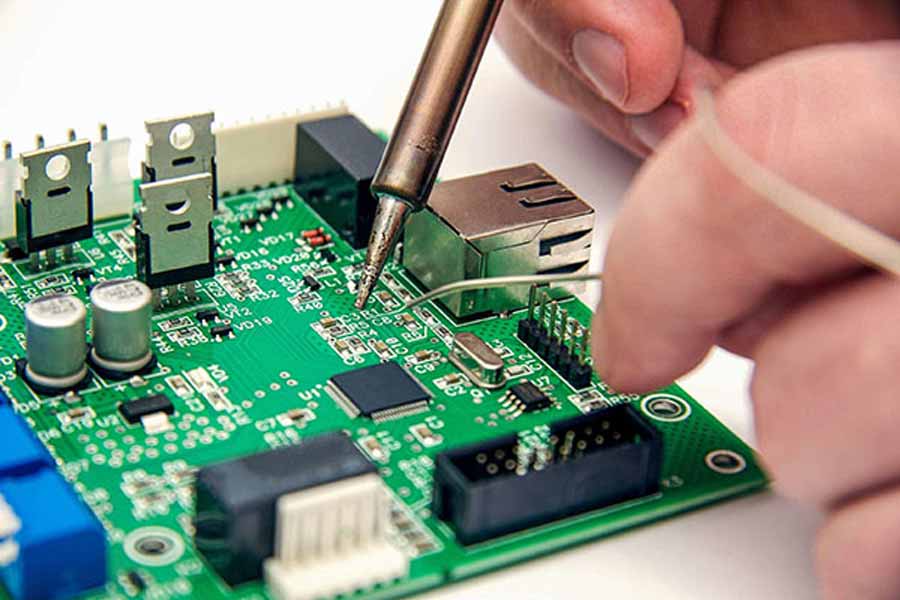
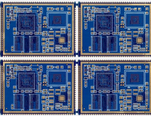
For PCB repair functions, given a large enough production lot or a long field life, a board will inevitably need maintenance. Rework before field usage is also critical, and some amount during manufacturing is always expected. In either case, technicians should be also to identify some of the common modes of failure for PCBs to more quickly and effectively reduce downtime for boards and return them to operation.
Soldering: Your First Check During PCB Repair
One of the first things to assuage to determine the function and robustness of a board is the quality of the solder work. The solder is the basis of the long-term union between the components and bare board. Poor solder technique or misapplication will be responsible for many issues during testing or later in a board’s lifecycle.
Solder application: Poor solder joint formation can lead to numerous issues. Poor/missing connections, lackluster solder coverage, bridging between pads, and other defects can usually be corrected with the reapplication of a soldering iron to create better joints. Excessive rework and heat application can lead to further issues such as pad lifting, which carries its own complications of electrical connection.
Solder cracking: The solder can develop cracks due to multiple thermal cycles or a cold joint during soldering work. Additionally, RoHS efforts have led to lead-free solder alloys with reduces plasticity, which leads to crack formation and propagation. Loose solder and components can bridge other connections and cause further damage. Common chip package designs are available with metal terminations to reduce the stress on the board during flexure.
Components Will Wear, So Be Prepared
During assembly, the completed bare boards accepted for further manufacturing will be populated with components according to the relevant design document. Often at this stage, a pick-and-place machine will place SMT components according to a plot of all the horizontal and vertical location data specified in the documentation output. Component-focused repairs can begin to surface at this point:
Misplaced components: This error can be perpetuated from the design level and missed during a review, or it could arise organically during placement. Suppose the misplaced component can solder down on the pads. This case could either result in a noticeable and extreme failure or a more subtle and insidious form of malfunction. Without obvious signs of failure, a component may operate but produce entirely nonsensical signals. Worse still, if these function as inputs elsewhere in the circuit, it may be challenging to diagnose circuit behavior operating erratically, absent any logic oversights.
Component failure: This situation could be due to a part that fails in the field or is missed during quality assurance. Depending on the level of failure and the importance of the component to the overall design, issues may present themselves in a multitude of separate ways. Improper power delivery may result in logic runtime errors, which can be difficult to diagnose. Catastrophic component failure may be easier to find, especially if a highly visible failure mode accompanies it. In any case, components need to be replaced, and an investigation will ensure that underlying thermal or electrical delivery issues aren’t contributing to the device failure. Finally, boards in service for an appreciable amount of time may need to have components replaced simply due to age. These components met or exceeded the service life or cycle usage established by the manufacturer and required regular maintenance.
Remain Cognizant of Other Board Repairs
There are many ways for boards to fail besides components and the solder used to connect them. PCB design is a complex manufacturing process that requires multiple processing steps; even the most thorough design reviews cannot entirely account for the board’s experience in the field. That said, there are additional field failures that should be considered.
Trace disconnection: Although less common than component failure, it is still a possible route of board failure. Particularly thin traces may experience degradation due to wear, especially if they are not of a requisite thickness to handle operating current densities. Severe weather events without proper chassis grounding can also be a failure mode. In these extreme events, there is likely more damage than just trace disconnects. Traces can be reestablished via soldering or reballing that provides a conductive metal to flow over the path of the trace.
Environment-induced failure: Boards subjected to rugged environments will require some additional thought in layout design. High-temperature locales should feature plenty of spacing between components, especially power circuitry, and may require more active cooling solutions. Dust and other debris can choke ventilation and become a smoke or fire hazard, and high moisture levels resulting in condensates will wreak havoc on the exposed metal surfaces of a board. In all these cases, special care should be taken as to the board’s long-term fixture to protect against the field adequately.


