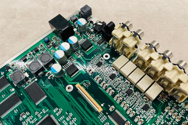
Within every single electronic device used today, there’s a printed circuit board (PCB) that makes it operate. The PCB is the heart of electronic devices, whether we’re talking about smart speakers for the home, your new intelligent thermostat, or the digital speedometer in your car. Of course, creating functional electronic devices requires much more than just throwing together a bunch of components and resistors.
The PCB assembly process is critical to get right the first time. A single misstep here could result in malfunctions, lack of functionality, or even the threat of accidents. In this post, we’ll cover some of the most important PCB assembly process steps and what you should know.
Understand the PCB Assembly Technologies
Assembling a printed circuit board requires more than just the raw components and a well-designed board. It also requires the right technology. In this case, there are several options to choose from, and each brings something different to the table. For instance, there’s surface mount technology (SMT), as well as manual soldering, and the use of pick and place machines.
While some PCB assembly processes will require just one technology, others will require a combination of two or more technologies. For example, many boards require the combination of through-hole technology (THT) and surface mount technology. Understanding when, where, and how to integrate those technologies is a critical consideration when choosing a company to handle your project or production.
It’s also important to understand that the PCB assembly steps involved with the various technologies differ, as well. Below, we’ve outlined some basic steps involved, as well as how they differ from technology to technology.
The PCB Assembly Process: An Overview
Solder Paste: If you’re following a traditional PCB assembly process, the first step is the application of solder paste. Note that this is not the case with THT, but SMT does require paste application and/or printing.
Component Placement: In the traditional PCB assembly process, the next step is to place the components on the board. This can be done manually, or it can be done with the assistance of machinery (pick and place systems). In THT assembly, components are placed by hand, which requires incredible precision. In the SMT process, robotic systems place components on the board. Note that automated placement is far faster than manual placement and is just as precise.
Reflow: In the traditional PCB assembly process, the next step is reflow, which is when the solder is first melted and then resolidified. The board and all its components move through an oven, which heats the solder, liquifying it and ensuring that connections are formed before the board moves into a cooler, where the solder is cooled.
Note that the THT process does not require reflowing solder. Instead, the second step here is to inspect the board and rectify component placement. This is due to the manual placement process – a visual inspection in conjunction with a design transport frame helps ensure placement accuracy.
In the SMT process, reflow soldering takes place at this time, as well. The board is sent through a furnace, which melts the solder paste, allowing it to flow as necessary, before the board passes through a series of coolers that gradually bring the temperature down, solidifying the solder on the board and cementing the components in place.
Inspection: The next step in the traditional PCB assembly process is a visual inspection of the board, soldering, and components. Note that this step has already occurred in the THT and SMT processes.
Through-Hole Part Insertion: The traditional process requires that through-hole insertion be done manually, after the reflow and inspection process. Soldering is also often done manually, but it may be done using wave soldering.
Wave soldering occurs during the THT process at this point, as well. The entire board moves over liquid solder and then moves through coolers to solidify the solder.
Note that there is no correlating step in the SMT process (it is actually already finished, and wrapped up after just three steps, although a visual inspection should still be conducted to ensure accuracy and to reduce the potential for errors).
Final Inspection and Cleaning: The final step in the traditional PCB assembly process is a final inspection of the board, the solder points, and the components, and a cleaning to ensure that debris or excess solder is removed.


