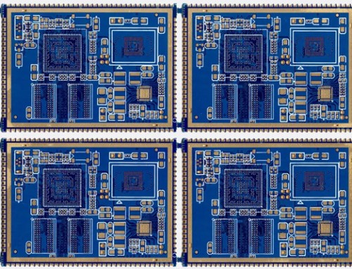
Aluminum Printed Circuit Boards (PCBs) have gained significant popularity in various industries due to their excellent thermal management properties, lightweight nature, and cost-effectiveness. However, achieving optimal signal integrity in aluminum PCB assembly is a challenging task that requires careful consideration of various factors. In this article, we will discuss some tips and best practices for achieving optimal signal integrity in aluminum PCB assembly.
Design Considerations
a. Track Width and Spacing: To ensure optimal signal integrity, it is crucial to maintain a proper track width and spacing. Wider tracks reduce crosstalk and parasitic capacitance, while narrower tracks may lead to signal degradation. It is recommended to use track widths and spacing as per the IPC standards for the specific application.
b. Layering and Stackup: The layering and stackup of the PCB play a vital role in achieving optimal signal integrity. It is advisable to use a multi-layer stackup with appropriate ground and power planes to minimize noise and ensure a stable signal transmission.
c. Routing: Proper routing techniques are essential to minimize crosstalk and signal interference. Avoid routing high-speed signals parallel to each other or near power lines. Use controlled impedance routing and maintain a consistent impedance throughout the signal path.
d. Shielding: To protect high-speed signals from external interference, it is recommended to use shielding techniques such as conductive coatings or enclosures. Shielding helps in reducing crosstalk and ensuring a cleaner signal transmission.
Material Selection
a. Base Material: Choose a high-quality base material with good electrical properties for the aluminum PCB. FR-4 or higher grade materials are preferred for high-speed signal applications.
b. Conductive Material: Select a conductive material with low resistance and suitable for the intended application. Aluminum is a popular choice due to its excellent thermal conductivity, but it may have higher resistance compared to copper. Consider using copper or gold plating for high-speed signal applications to ensure better conductivity.
Fabrication and Assembly
a. Drilling and Routing: Accurate drilling and routing are crucial for achieving optimal signal integrity. Use high-precision equipment to maintain tight tolerances and minimize signal degradation.
b. Plating: Proper plating of the conductive paths is essential to ensure good electrical connectivity. Choose the appropriate plating method, such as immersion gold or organic solderability preservative (OSP), based on the application requirements.
c. Component Placement: Carefully place components to minimize signal interference and crosstalk. Maintain adequate spacing between high-speed components and avoid placing them close to power lines or other high-speed signals.
d. Soldering: Use high-quality soldering techniques and materials to ensure proper electrical connections. Consider using surface mount technology (SMT) or through-hole components, depending on the application requirements.
Testing and Validation
a. DC Parameters: Measure and validate the DC parameters of the aluminum PCB, such as resistance, capacitance, and inductance, to ensure they meet the design specifications.
b. AC Parameters: Perform AC parameter testing, such as high-frequency signal analysis, to assess the signal integrity of the PCB. Use suitable test equipment and analyze the signal response, including impedance, phase, and delay.
c. Crosstalk and Interference Testing: Evaluate the crosstalk and interference levels between different signal paths on the PCB. Use appropriate test methods, such as crosstalk testing between adjacent traces or slots.
Achieving optimal signal integrity in aluminum PCB assembly requires careful consideration of design, material selection, fabrication, and testing. By following the tips and best practices discussed in this article, engineers can ensure reliable and high-quality signal transmission in aluminum PCB-based applications.


