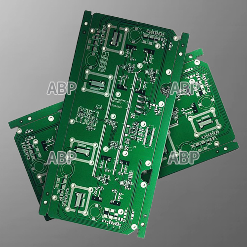
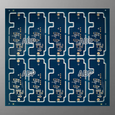
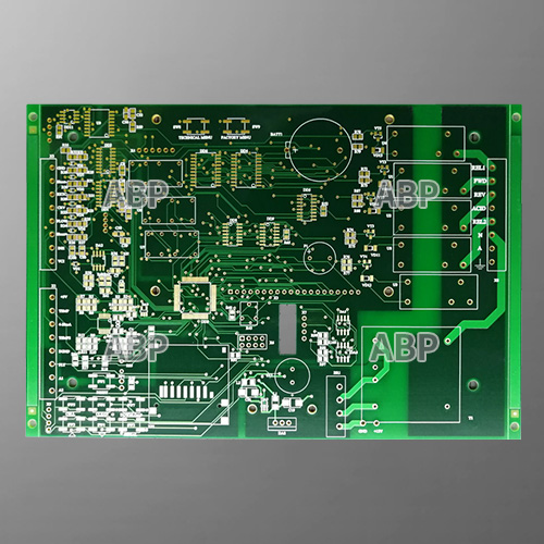
What is PCB Manufacturing?
Here at ABP, PCB service refers to full feature printed circuit board manufacturing service. With 17 years’ experience in PCB fabrication, we have handled hundreds of thousands of PCB projects, and covered almost all kinds of substrate materials including FR4, Aluminum, Rogers, etc.
Specialize in PCBprototype over 10 years
Prototype PCB lead time as quick as 24 hours
The most favorable price in whole industry
Quick turn PCB assembly turnkey services
Start your PCBA order from 1pcs
On-time delivery by DHL & FedEx
Professional technical team provide one-to-one service
Professional QC team, 100% Guaranteed quality
Prototype Printed Circuit Boards Meet High-Quality Standards
ABP offers rapid PCB prototyping services for quick-turn PCB at high quality and low cost. We’re fully compliant with ISO9001:2008 quality management systems, and we have an in-house quality control department to verify that all work meets each regulation depicted by the high standards.
Depending on your custom requirements, we can prototype your PCB within 3-7 days, compared to 6-18 days of Standard PCB service.
Check out our circuit board prototype capabilities in the following table:
| Item | Capability |
|---|---|
| Layers | 1-30 |
| Thicker Copper | 1-6OZ |
| Products Type | HF(High-Frequency)&(Radio Frequency) board, Impedance controlled board , HDI board ,
BGA& Fine Pitch board |
| Solder Mask | Nanya&Taiyo ;LPI & Matt Red, green, yellow,white, blue,black. |
| Base material | FR4(Shengyi China、ITEQ, KB A+,HZ), HI-TG, FR06, Rogers,Taconic、Argon and so on |
| Finished Surface | Conventional HASL,Lead-free HASL,Falsh Gold, ENIG (Immersion Gold)OSP(Entek), Immersion Tin,ImmersionSilver,Hard Gold |
| Selective Surface Treatment | ENIG(immersion Gold)+OSP, ENIG(immersion Gold)+Gold Finger,Flash Gold +Gold Finger,
immersion Silver+ Gold Finger, Immersion Tin+Gold Finger |
| Technical Specification | Minimum line width/gap:3.5/4mil(laser drill) Minimum hole size:0.15mm(mechanical drill)/4mil(laser drill) Minimum Annular Ring: 4mil Max Copper thickness: 6OZ Max Production size:900×1200mm Board Thickness:D/S: 0.2-7.0mm, Multilayers:0.40-7.0mm, Min Solder Mask Bridge:0.08mm Aspect ratio: 15:1 Plugging Visa capability: 0.2-0.8mm |
| Tolerance | Plated holes Tolerance:0.08mm(min±0.05) Non-plated hole tolerance:0.05min(min+0/-0.05mm or +0.05/-0mm) Outline Tolerance:0.15min(min±0.10mm) Functional test : Insulating resistance : 50 ohms (mormality) Peel off strength: 1.4N/mm Thermal Stress test :2650c,20 seconds Solder mask hardness:6H E-Test voltage :500V+15/-0V 30S Warp and Twist: 0.7% (semiconductor test board≤0.3% ) |


